Organic and perovskite photovoltaics are the solar cell research fields with the greatest interest from the community. Many articles are published each week about it and for this reason, I will certainly write a lot about those two kinds of solar cells. Here I chose to present how do Organic Solar Cells work.
Organic Materials?
The particularity of organic solar cells in comparison with silicon solar cells is the use of organic semiconductors. Many advantages are related to organic materials and the greatest is their price. Organic materials are abundant and easy to process. Thus organic solar cells are a low-cost technology to harness solar energy. In addition, the weak intermolecular Van der Waals interactions in organic materials enable to process them with a large variety of techniques, notably thin films on the large surface. Many of the processes are easy to carry out (in comparison with silicon that has to be purified, that is very expensive and energy-consuming). That allows organic solar cells to be coated on flexible substrates with very large areas.
Moreover, organic materials are significantly attractive because they usually have a high absorption coefficient combined with high transparency. Their properties are also tunable with efficient solution processes.
Therefore organic materials are very versatile in term of processing methods, in term of substrates and in term of applications. For many reasons, including stability under direct sunlight, organic solar cells researchers now channel their efforts into indoor applications.
The photoelectric materials
In such solar cells, the active layer is composed of amorphous organic materials with semiconductive properties. These materials are often conjugated polymers. Conjugation may be described as the overlap of p-orbitals that leads to the delocalization of pi-electrons across the chain of aligned p-orbitals. The absence of any crystallographic structure, compared with inorganic materials that wring their semiconductive properties out of their crystallographic structure, leads to a low dielectric constant (εr=2-4). Thus it results in tightly bonded excitons (electron-hole pair). The Frenkel exciton binding energy is comprised between 0.3 and 1eV: that is large and it prevents exciton dissociation by an electrical field.
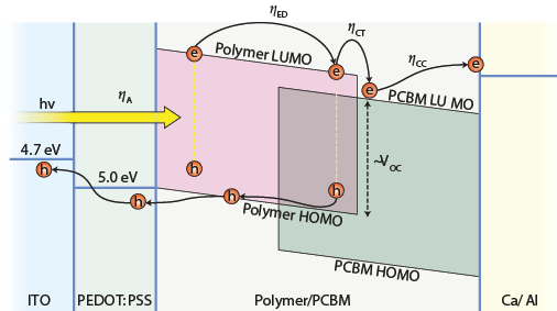
The active materials were firstly designed by Dr Ching W. Tang from Kodak in 1979 by superposing two layers of n and p-type semiconductors, as it was done with silicon. Researchers used to process donor-acceptor bilayer planar heterojunctions that achieved 1%PCE. Do to so, the energy difference between the LUMO (lowest unoccupied molecular orbital) of the donor material and the HOMO (highest occupied molecular orbital) of the acceptor leads the dissociation of Frenkel excitons when absorbing light. Then, the separated holes and electrons are collected to the anode and the cathode respectively. However, such planar structures had many issues scientists had to deal with. The main was that for such planar junction, the surface area between the donor and acceptor interface was tightly restricted and the carrier lifetime was too small so that the electrons and holes could recombine before reaching their respective electrodes.

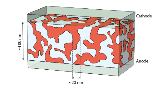
That leads in 1995 to the development of bulk heterojunctions, simultaneously with polymer-fullerene by Prof. Alan Heeger in UC Santa Barbara and with polymer-polymer blends by Prof. Sir Richard Friend in Cambridge University. Bulk heterojunction involves the mix of a donor and acceptor materials as an active layer. As shown on the figure, distances electrons and holes have to travel before being collected are much reduced and the surface of such nanostructured materials is largely enhanced. That lead to much higher performances.

The architecture
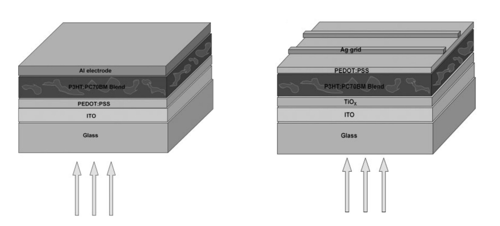
Traditional structures were made using the model of silicon solar cells in which the photons were going through the anode before being converted to exciton in the bulk heterojunction. However, it has been shown that an inverted structure behaves much better and was more stable.
The working principle of these cells is very easy: in the Bulk heterojunction, incident photons are absorbed, that leads to the creation of an exciton. These excitons can diffuse within the material, before being separated as a hole-electron pair. Each carrier is transported to a transport layer toward its respective electrode.
The bulk heterojunction is composed of a donor polymer, P3HT for example and an acceptor organic material. Owing to their strong electronegativity and high electron mobility, C60 derivatives like PCBM have become standard acceptor molecules in OPV devices. Today, the inverted structure with fullerene derivatives has become a standard in organic solar cells.

Research perspective
Since the advent of perovskite solar cells, many researchers in the field of organic photovoltaics have drifted to this new field. That lets much fewer resources to the organic field. However, This is now a much mature technology. Scientists focus on ensuring their stability and improving their efficiency. Many companies are trying to commercialise it, including Eight19 in Cambridge (UK) and Armor in Nantes (France). Their developments may become great commercial hits in the coming years depending on what they chose as market segments.
The figures are from Ameri T. et al. and Chen L.M. et al.
 0000-0002-6484-2157