Julien Barrier
Max Planck Research Group Leader
Low-Dimensional Electronics
MPI-FKF, Stuttgart
 0000-0002-6484-2157
Research Interests
My research group at the Max Planck Institute for Solid State Research uses electronic transport in graphene-based van der Waals heterostructures to study how electron-electron interactions shape quantum matter in low dimensions. The ability to stack crystalline layers free from lattice-matching constraints, to control the twist angle between them, and to place gates and screening layers a few nanometres from the active region lets us set the dimensionality, the coupling and the interaction strength of a system inside a single device, instead of comparing samples that differ in disorder and geometry. We follow three connected directions.
- Electronic transport in two-dimensional graphene, Rev. Mod. Phys. 83, 407 (2011) [arXiv:1003.4731] [DOI]
- Van der Waals heterostructures, Nature 499, 419–425 (2013) [arXiv:1307.6718] [DOI]
- Moiré nano-optoelectronics, 2D Materials 13, 021501 (2026) [DOI]
One-dimensional electronic channels
When two graphene layers are stacked with a minute twist, the lattice reconstructs into domains of alternating Bernal (AB and BA) stacking, separated by domain walls. These twist domain walls host protected one-dimensional (1D) channels. Our first experiments showed that they are ballistic, single-mode conductors, with a conductance reaching 4e²/h and a width below 3 nm. The channels are gate-controllable and can be made chiral or non-chiral, depending on whether a magnetic or an electric displacement field opens the gap in the surrounding domains.
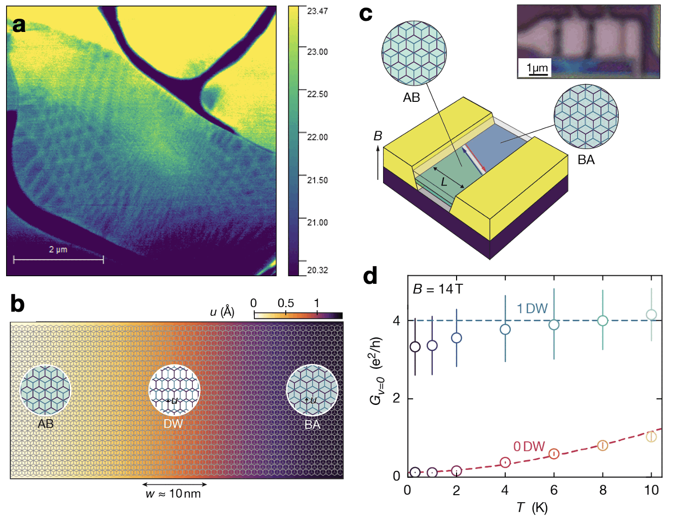
In one dimension, electrons cannot be described as weakly perturbed free particles. The system becomes a Tomonaga-Luttinger liquid, whose properties are set by a single interaction parameter. Most experiments have measured this parameter in samples where material and geometry fix its value. We use domain-wall channels, together with the screening technique described below, to make interaction strength a variable. We ask what a single 1D conductor does as interactions are tuned, and what happens when several channels are coupled into ladders, networks, or pairs that can only exchange momentum through Coulomb interactions. This is a clean setting in which to ask when and how one dimension turns into two.
Recent articles on the topic:
- One-Dimensional Proximity Superconductivity in the Quantum Hall Regime, Nature 628, 741 (2024). [arXiv:2402.14451] [DOI] [PDF]
- Long-Range Ballistic Transport of Brown-Zak Fermions in Graphene Superlattices, Nature Communications 11, 5756 (2020). [arXiv:2006.15040] [DOI] [PDF] [SI]
Coulomb screening and interaction engineering
The textbook picture of non-interacting electrons breaks down in the presence of strong Coulomb repulsion, giving rise to collective many-body phenomena that are notoriously difficult to predict. A key methodological contribution of my work is the use of van der Waals heterostructure-based screening to control Coulomb interactions in situ. A metallic layer placed within a few nanometres of a two-dimensional system reduces the strength of the interaction without altering doping, strain or chemistry. By thinning the spacer layer by layer, the interaction strength can be reduced progressively, and by decoupling the screening layer from the sample through a twist, it can be pushed an order of magnitude beyond conventional screening designs.
With this approach we showed that proximity screening greatly enhances the electronic quality of graphene, and that screening suppresses the superconducting phase of magic-angle twisted bilayer graphene, which points to a pairing mechanism driven by electron-electron interactions rather than phonons. The same strategy has revealed other correlated phases in a strongly interacting electron-hole Dirac plasma in monolayer graphene that produces giant magnetoresistance. Together, these results establish interaction tuning as a unifying experimental strategy for mapping the phase diagrams of correlated quantum materials.
Recent articles on the topic:
- Coulomb Screening of Superconductivity in Magic-Angle Twisted Bilayer Graphene, Physical Review X 16, 031040 (2026). [arXiv:2412.01577] [DOI]
- Proximity Screening Greatly Enhances Electronic Quality of Graphene, Nature 644, 646 (2025). [arXiv:2507.21997] [DOI]
- Giant Magnetoresistance of Dirac Plasma in High-Mobility Graphene, Nature 616, 270 (2023). [arXiv:2302.06863] [DOI]
Josephson junctions
Josephson junctions are a natural way to probe superconducting correlations in a low-dimensional channel, and they are also what led us to the 1D channels above. We were originally looking for ways to build junctions from quantum Hall edge states, which is difficult because the edges must come within the superconducting coherence length of the electrodes. Twist domain walls solved that problem. Junctions based on these channels carry a supercurrent that persists in high magnetic fields and is limited only by the quantum of conductance of strictly 1D channels. They are gate-controllable and show Fabry-Pérot resonances, much like superconducting quantum dots.
My group builds on this platform to use Josephson junctions as probes and as devices: to study how superconductivity enters a single 1D channel (be it a quantum Hall edge, an anomalous quantum Hall channel or an AB/BA domain wall) how it behaves when interactions in that channel are tuned by screening, and how it is shared between coupled channels.
- One-Dimensional Proximity Superconductivity in the Quantum Hall Regime, Nature 628, 741 (2024). [arXiv:2402.14451] [DOI] [PDF]
Complementary probes
Alongside electrical transport, I have worked on nanophotonic, photocurrent and non-linear transport techniques, mostly in collaboration with F. Koppens (ICFO). They give access to quantities that dc transport cannot measure. We used IR and THz photocurrent to show that magic-angle twisted bilayer graphene hosts spontaneous inversion symmetry-breaking correlated states, mapped the formation of moiré minibands with optical spectroscopy, and demonstrated single-photon detection in a bilayer graphene superlattice using negative differential conductance. We use these probes selectively where they answer a question that transport alone cannot. These probes generalise to non-linear transport, in which out-of-equilibrium physics can be probed, highlighting bandwidth-limitations.
Recent articles on the topic:
- Bandwidth-Limited Critical Currents in Electrically Tunable Moiré Bands, Nano Letters (2026). [arXiv:2607.01056] [DOI]
- Single-Photon Detection Enabled by Negative Differential Conductivity in Moiré Superlattices, Science 389, 644 (2025). [arXiv:2505.13637] [DOI]
- Terahertz Photocurrent Probe of Quantum Geometry and Interactions In Magic-Angle Twisted Bilayer Graphene, Nature Materials 1034 (2025). [arXiv:2406.16532] [DOI]
- Infrared Spectroscopy for Diagnosing Superlattice Minibands In Magic-Angle Twisted Bilayer Graphene, Nano Lett. (2024). [arXiv:2404.05716] [DOI]