 0000-0002-6484-2157
The properties of crystalline semiconductors, and particularly those giving rise to the photoelectric effect, are mainly due to the presence of defects inside a crystalline lattice. Two weeks ago, at the annual Perovskite Solar Cells and Optoelectronics Conference (#PSCO17) in Oxford, one of the main topic developed was the exceptional defect tolerance found in the perovskites and the doping allowed by it. I contacted Prof. Aron Walsh, from the Department of Materials at Imperial College London (United Kingdom) that published recently a an interesting commentary in Nature Materials: ‘Instilling defect tolerance in new compounds’ and presented new results at the conference.
The role of defects in crystalline semiconductors
There are different type of defects in crystalline semiconductors: interruptions (crystallographic defects) or foreign atoms in the lattice (impurities). Those interruptions can be present in the form of point defects, including atomic vacancies, interstitials or anti-site substitutions, and higher dimensional defects like dislocations, grain boundaries or precipitates. Defects are formed in the lattice because there are thermodynamically favourable: their equilibrium concentration depends highly on their formation energy.
All of these defects will have different impact on the electronic and optoelectronic structures. Defects with energy levels inside the bandgap will induce electron or hole trapping. In other cases, defects can imply electron or hole emission: one hole and electron can be captured by a recombination centre. To sum it up, defects in a crystalline lattice produce recombination or emission centres that are at the heart of the optoelectronic properties of a lattice.
Due to these defects, semiconductors create unintentional n- or p-type doping, leading to the formation of p-n junctions. Also, from Fermi level pinning by defect states, unfavourable band alignment can be created that limit the voltage of solar cells.
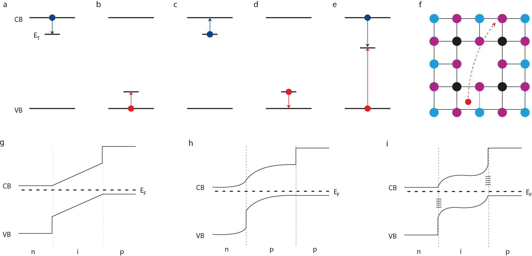
Defect tolerance properties within perovskites
Perovskites are also crystalline semiconductors. For this reason, defects exist and are active within the lattice. Their implications are not negligible and contribute significantly to many properties like carrier recombination. Also, in some cases, the presence of defects seems to have no major implication on recombination that leads to astonishing performance of perovskite solar cells. Prof. Aron Walsh explains this defect tolerance:
Practically speaking, in halide perovskite we expect many point defects to be present, but they do not destroy the performance of solar cells. In optoelectronic devices, it is essential to avoid non-radiative processes that convert electronic to thermal energy via defects. These events lower efficiency and can trigger device breakdown. It turns out that many of the low energy point defects in halide perovskite are “inert”, which is one of the reasons for the materials success. In other technologies such as kesterite (Cu₂ZnSnS₄) solar cells, non-radiative recombination is high, limiting the solar cell efficiencies to below 15%. Such defect intolerance is common in many materials that have been studied for solar cells (e.g. SnS, Cu₂O, FeS₂), which is why the unusual behaviour of halide perovskites is so important to understand.
I think that understanding the reason leading to such properties will lead to ways to enhance not only the properties of perovskites, but also the properties of other semiconductors. That is one of the reasons why research with perovskite is of high importance.
There are other properties that are in relation with the presence of defects. The mobile ions issue, which was previously discussed on this blog, is said to be due to the defect properties within perovskite structures. The presence of halogen interstitial or vacancy within the structure plays a major role: it has been observed that under light exposure, iodide and bromide species migrate along the cell, creating iodide- and bromide-rich domains, that act as recombination centres. Many scientist think that improving the crystal quality would lower the separation in halogen-rich domains. Personally, I think that a better understanding of the defect tolerance will allow us to develop better materials, that will not present hysteresis cycles lowering the performance of the cell.
Doping the perovskites
In typical crystalline semiconductors, defects are very important for the reason they allow the doping of the structure. Doping means that a given material can be tuned to be a better electron- or hole-acceptor, due to the presence of charged defects. Therefore, the question arises as to whether the perovskite materials can be tuned or not. That is a real question. Aron has an enticing opinion on it:
In principle, doping of perovskite is simple: partial substitution of Pb²⁺ by a metal with a higher charge could generate excess electrons, while replacing it by a singly charged metal could generate excess holes. The challenge is achieving this without forming other defects that compensate the charge.
He explains the process in a clear and precise manner in his latest publication, even which there are now limitations. Working with these limitations, and trying to overcome these are a challenge most of the scientists in the perovskite community are working on.
Going further with p-n junctions
If one manages to dope perovskite with tangible results, these could lead to the creation of p-n junction and therefore to field-effect transistors made with perovskite. The perspective of Prof. Walsh is very interesting at this point:
It will be possible once we would have understood how to control defect concentrations and transport. The current generation of perovskite solar cells are based on a p-i-n architecture, where the perovskite layer is intrinsic (i) with low carrier concentrations. Alternative p-n junctions would enable lower cost perovskite devices with fewer layers of materials, and potentially higher efficiency comparable to the best silicon solar cells. If realised, this would be a major breakthrough in the field.
Thus, the challenge to address is of great importance. I am sure we will understand in the year ahead the main reasons why perovskite are defect-tolerant, and will find solutions to create p-n junctions that will improve both the quality, the performance of solar cells, but also will allow us to create new electronic devices based on perovskites that will revolutionise the semiconductor industry.
The figure has been drawn by James M. Ball and Prof. Annamaria Petrozza for their Nature paper.