 0000-0002-6484-2157
I started this blog two months ago to share my opinion and enthusiasm about third generation photovoltaic technologies. In fact last year I used to ask questions to some of my teachers about perovskite solar cells, and each time, they were very sceptic about it and told me that the topic exploded some years ago, but that it could rapidly fall back. In the field, we call it the Perovskite Fever. I have never agreed with the fact perovskites could easily fall back, telling this was the original aim of this blog. In this perspective, I give my opinion about the past, current and future developments of perovskite solar cells and my vision on how to push it further.
Historical background: the Perovskite Fever
The perovskite technology has received tremendous interest in photovoltaic applications for five years. At the very beginning, this material was tin-based and its semiconducting properties were reported in 1994 by Mitzi et al. Actually, in 2009, Miyasaka et al. were the first to use perovskite materials into solar cells. At the time, they used lead-based perovskites in DSSCs to enhance their properties. Later on, in 2012, Kim et al. employed an all-solid configuration, reporting a 9% efficiency.
Since then, the topic received substantial attention from researchers all around the globe. Hence the performance of perovskite solar cells has been dramatically improved to more than 20% efficiency, boosted by material and interfaces engineering. Today, I consider perovskites as one of the most promising semiconducting material, that will boost the realm of optoelectronics in a very near future. Its low processing cost, abundance and excellent optical properties including a high absorption coefficient, strong photoluminescence, low trap-state density and long carrier diffusion length make it a perfect candidate for applications in solar cells, lasers, light emitting diodes, etc.
The crystalline structure
Before trying to talk about future developments, I think it is very important to understand the crystalline structure of perovskite. The term perovskite originated from the similarity with the CaTiO3 mineral, called Perovskite. In this structure, usually referred as ABX3 perovskite, a divalent metal B (lead in optoelectronics applications) is surrounded by six halogen atoms (iodide or bromide) in an octahedral network, and the cation A (methylammonium, formamidinum or caesium) is either located in the centre of an eight BX6 octahedral network (3D perovskite) or sandwiched between corner-sharing BX6 octahedral layers (2D perovskite). In fact, each layer of BX6 octahedra is only connected to each other by weak van der Waals forces. This structure is very important to understand because all the physical properties are induced by the crystallographic lattice.
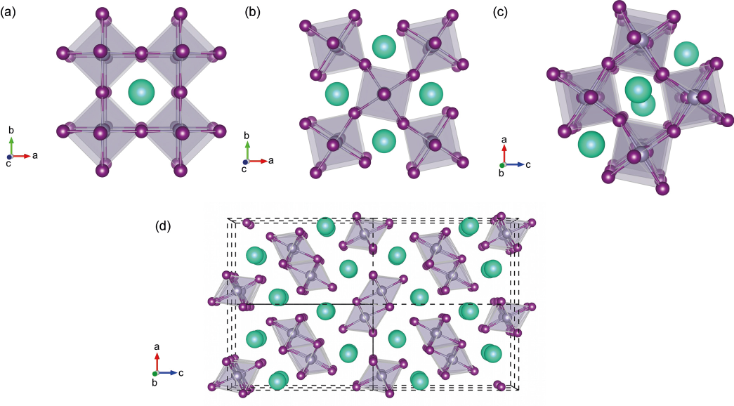
It has recently been demonstrated that this crystalline structure evolves with the temperature. One must understand the phase dynamics leading to different lattice structure. Below 150K, lead halide perovskites are stable in an orthorhombic phase (Pnma). Behind 150K, the tetragonal phase (I4/mcm) is more stable and at room temperature or higher, the cubic phase is stable (Pm3̅m). Only the cubic phase presents optoelectronic properties. It means that at low temperature, the perovskite cannot absorb or emit light. However, there is no clear transition: some scientists predicted metal halide perovskites to be metastable: particularly between 200 and 300K, both the tetragonal and the cubic phases can coexist. It is a problem to address: if this material cannot be represented on an equilibrium phase diagram, it means it can only be synthesised with a finite lifetime.
The lattice evolves
The metastability is often associated with a very small energy barrier for the cation rotation. It has been predicted that molecular sub-lattice is dynamically disordered due to the ability for the cation to rotate, but scientists found that Bragg scattering does not probe such a local disorder, even if these vibrations are observed with the vibrational IR and Raman spectra. That lets a bunch of physical and chemical properties to understand.
Ion migration processes are also of utter importance. In fact, there are charged point defects in the bulk that allow the transport of ions, thus ensuring spatial fluctuations of the electrostatic potential of the solar cells. Schottky defects are prevalent in the crystallographic structure. Therefore it has been observed with X-ray diffraction that the ions segregate into crystalline phases under illumination: one iodide rich and one bromide-rich. The accumulation of charge carriers in different zones increases the lattice strain and is a path toward more and more segregation. That “doping” leads to a hysteresis cycle of the IV-curve, that reduces the photovoltaic performance. However, this is a reversible process. That means that in the dark, the iodide- and bromide-rich phases blend one each other. To date, the mobile ion issue is the one to address in priority before commercialisation. A way to find solutions is to focus on the crystallisation process, that is still unknown. Understanding this will surely lead to more reproducible, better performance solar cells, and will mitigate the hysteresis issue, providing greater assets to address the problem of long-term stability. During the crystallisation process, the role of chloride ions remains still unknown. It could be the source of a doping effect that would explain the large carrier diffusion length of perovskites because it is challenging to find chloride ions in the final perovskite. The reduction of ion diffusion is also important: the understanding of doping processes and exciton confinement will allow scientists to understand the dopant states and the impact of halide ion exchange.
The crystalline structure and the lattice vibrations drive directly the degradation of the materials. Even if there have never been any rigorous attempts to model the decomposition path of hybrid perovskites, including chemical reactions, anharmonic lattice vibration and thermal conductivity, many scientists are on their way. I think these are important things to be understood for the sustainability of the perovskites.
The electronic properties
All of the lattice behaviour changes the electronic properties, and particularly the electron-hole recombination. There are three types of possible recombination: non-radiative, radiative, and Auger recombination. Only the non-radiative recombination limits the efficiency of the solar cells, according to the Shockley-Queisser law. Hence the efficiency of perovskite solar cells is important due to the low number of non-radiative processes.
Moreover, a lot of work to understand the electronic properties have been carried out by simulations and theoretical calculation, often based on first principle calculations. These simulations allow scientists to compare different models and therefore to identify the crystalline structure based on measurable deductions. It has been shown that the valence and conduction band structure are quite sensitive to changes in the crystal structure. The band are also perturbed by the vibrations of the lattice and electron-phonon coupling, that increase the rate of non-radiative recombinations, thus decreasing the efficiency of the solar cells.
Furthermore, there are defect levels in the bandgap, and working further on finding and reducing these levels can allow scientists to understand the low rate of non-radiative recombination. I am sure that this will have a broad impact in solid state physics.
Another field of deep interest lie at the surfaces, the grain boundaries and the interfaces of perovskites. A lot of work has currently been achieved by many scientists to understand the influence of these parameters in the device performance and to push its limit further in terms of long-term stability.
Moving towards luminescence
Applications for perovskites have started in the solar cells field, but the research realm is moving to other optoelectronic properties. The first is light emission allowed by metal halide perovskites. Working in this field is very important because these properties are due to radiative recombination. Enhancing the radiative recombination would enhance both the absorption and emission properties of the cells. That may seem counter-intuitive, but the perovskite solar cells that would present the best performances will also emit light when working.
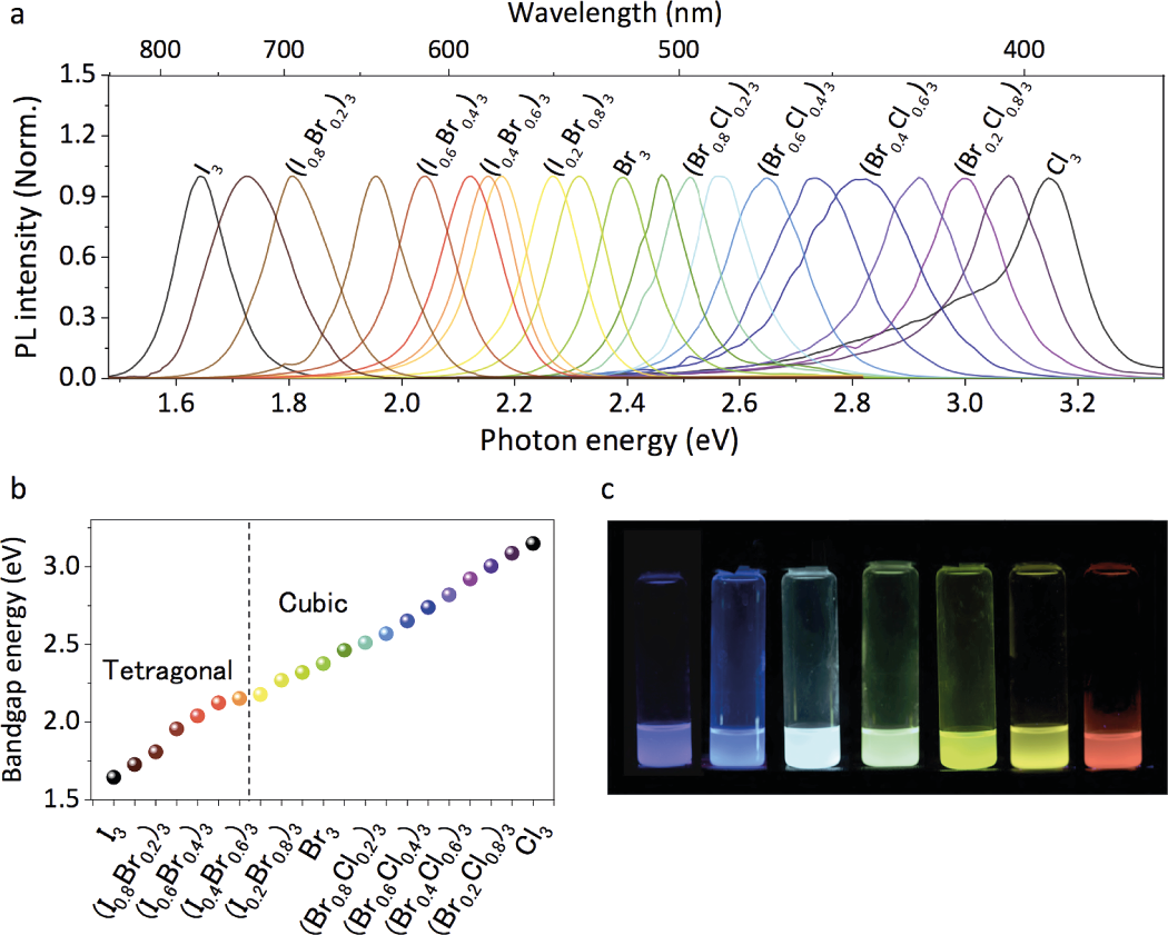
Thus the optical properties, including tunable emission are important within perovskite solar cells. As we just saw, the material presents excellent exciton and carrier properties, leading to a high performance in the solar cell research area. The same properties make it an outstanding light emitter that can be used in LEDs and lasers. If we compare it with conventional III-V and II-VI semiconductors, an attractive feature of perovskite is the ability one can have to tune the emission wavelength, throughout the whole visible range. This can be achieved by controlling the stoichiometry, by substituting halide elements, for example, chloride or iodide. Replacing lead by other metal ions also enable a bandgap tuning, that can be achieved in the near infrared or ultraviolet.
Electronic properties of luminescence
Perovskites are excellent light emitters. Their high quantum efficiency is the result of a clear bandgap with a low rate of charge-trapping states, that promotes the exciton radiative recombination efficiency. Some scientists have discussed how the unique electronic band structure of these perovskites contribute to the formation of defect-tolerant CsPbX3 nanocrystals. One of the future challenges in modifying optical properties is by doping the crystals with Mn2+ or Bi3+, creating heterostructures with metal nanoparticles.
Luminescence has been mostly observed in perovskite nanocrystals. In fact, in that crystal the quantum confinement effect — described by a crystal size that is too small to be comparable to the Bohr radius of exciton — allows the energy levels to be discrete (instead of continuous as in solids). Thus, the optical absorption and emission properties can easily be tuned by changing the size of the semiconductor, i.e. the nanocrystal. Hence, when reducing the size of the nanocrystal, scientists have observed a blue shift in the bandgap. If most of these effects have been observed in all-inorganic CsPbBr3 perovskite nanocrystals, the improvement of this structure and use in hybrid halide perovskites will surely lead to enhancement of the absorption properties of perovskite solar cells.
Main applications in light emission
There are two main applications for luminescence with perovskite: optical lasing and light emitting diodes. Due to the high absorption coefficient and strong photoluminescence properties, optical lasing is possible. In fact, when a high gain material is put in an optical cavity, one can expect lasing. Exploration of amplified spontaneous emission in perovskite allowed scientists to design some perovskite-based lasers. We understood in this perspective that the high crystallinity of perovskites was the base of many properties. Here, nanocrystals can act as a Fabry-Pérot cavity, allowing lasing in the materials. This will lead to applications in nanoscale optoelectronics, with the ability to tune the emission wavelength to achieve lasing in the full visible spectrum.
Light emitting diodes applications make perovskite one of the most promising material. The fact it is low cost, easy to prepare, with high performance and a high colour tunability, with very precise emission rays make it a technology we will hear about in the coming years. The main issue is overcoming the stability issue. I am sure that a combined work from two different communities (the one that works on solar cells and the one working with LEDs) will be the key towards these applications.
Forthcoming challenges
I do not think that the compound design should be application-driven. Perovskite is truly a multifunctional semiconductor, and the understanding of its properties for particular applications should drive the design for the whole applications. The understanding of the functions of each component, such as organic cations, metal halide octahedra network, and effect of each on the entire crystal structure in order to formulate better compound for each application is of paramount importance.
One of the biggest challenges for metal halide perovskite is their stability. Their vulnerability surrounding environments, such as moisture and oxygen or polar molecules, affect dramatically the performance of the devices. This casts a shadow towards their practical applications and commercialisation. Thus we need to develop a method to stabilise the material, both by chemical approaches, (capping agents, for example, stabilisers) or by physical methods such as device encapsulation.
Perovskite may have reached their high development peak, but we saw in this perspective there is still many years of research for chemist and physicist to improve the optical and electronic properties of perovskite by tailoring the crystallographic sciences and designing new devices. I think we are at the beginning of a new Perovskite era when scientists will not try to improve their devices based on existing knowledge of organic and inorganic semiconductors but will try to deeper understanding. And there is plenty of room for this!
I am deeply convinced that the world rapidly needs stable, efficient and low-cost photovoltaic solutions. Tackling climate change is a matter of days. A better understanding of Perovskite emission properties and their degradation mechanism will lead to a better understanding of this incredible material, that makes the Perovskite Fever not over yet. I am sure that we will understand all of their physical properties so that Perovskites will power what will become the major source of energy within 10 years, and I have a glimmer of hope that Perovskite will lead us to a sustainable future.
The Perovskite structure illustration has been drawn by Walsh et al., the luminescence illustration by Pathak et al.